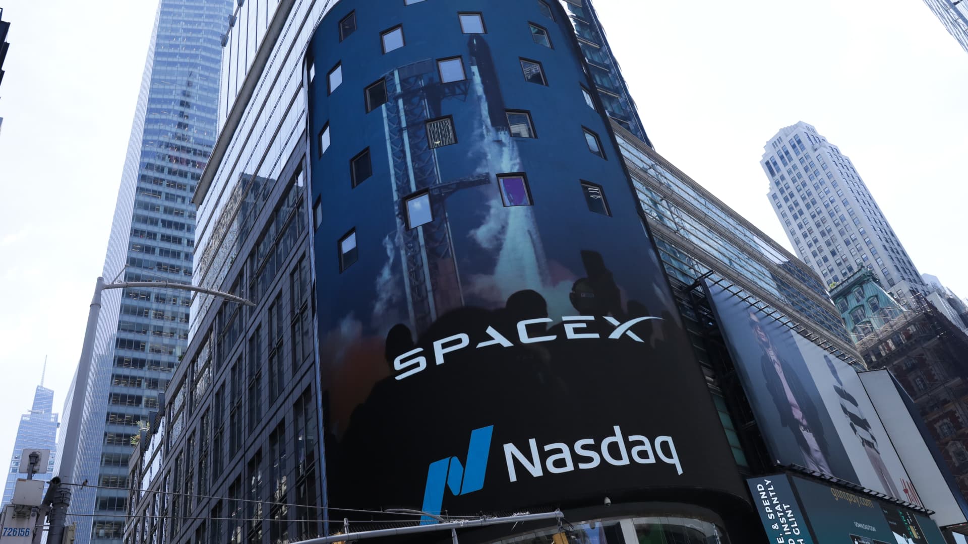
Nvidia has committed at least $6.5 billion into companies developing photonics technology in the past three months, as the company races to invest in solving one of the major bottlenecks to the rollout of AI.
Photonics, the use of light to transmit data, is an emerging technology considered to be a more efficient alternative to the current process of transferring data using electricity. Electrical data transfer consumes more energy — a factor which is increasingly seen as a blocker to the broader deployment of AI.
Since the beginning of March, Nvidia has announced $2 billion investments into Lumentum, Coherent and Marvell, all of which are developing photonics tech. The chip giant also said it would invest $500 million into Corning to develop advanced optical connectivity solutions, and participated in optics startup Ayer Labs’ $500 million Series E funding round.
“Photonics represents a way for Nvidia to scale their AI infrastructure without the energy costs that staying with electrical and copper will incur,” Alvin Nguyen, senior analyst at Forrester, told CNBC.
“By investing in photonics companies, Nvidia is making sure that advancements in photonics continue and it will prevent them from hitting a scalability and performance wall that will occur if they remain on electrical and copper.”
Solving bottlenecks
Photonics can be used in AI infrastructure by using light to move data between graphics processing units (GPUs), memory, networking chips, servers and data centers, instead of relying only on electrical signals running along copper.
While copper is the main connectivity standard today because of its lower cost and high reliability, photonics will become more prominent in AI infrastructure over time, Brian Colello, senior equity analyst at Morningstar, told CNBC.
“Nvidia’s roadmap of next generation AI rack-scale solutions will require an increasing amount of optical connectivity to process the exponentially rising bandwidth with new models and higher usage,” he said.
The chip giant has already made some photonics tech available as part of its networking solutions offering, with the company announcing tools that it said will enable AI factories to connect millions of GPUs across sites while drastically reducing energy consumption and operational costs.

“When you look upstream, you come to the conclusion that we’re starting to scale our silicon photonics technology,” Nvidia CEO Jensen Huang said at the GTC in March, pointing to Nvidia’s ethernet networking platform used to connect AI factories and GPU clusters. He also said the company was starting to add photonics to its GPU-to-GPU interconnect technology.
“Which means the amount of silicon photonics technology capacity that we need is substantially higher than the world has today,” he added. “So we work with the supply chain to make sure we can help them build up the capacity in advance of that.”
Lumentum’s stock has risen 134% since the start of the year, while Coherent is up 96%. Marvell has seen its shares increase by 122% in 2026 and Corning 111%.

Shares of companies involved in photonics have soared in the past year.
Nvidia is one of the many AI stakeholders recently making the move to funnel cash into photonics tech.
Chipmaker AMD joined Nvidia in the Ayer Labs round, as well as acquiring startup Enosemi in 2025, alongside making equity investments in Teramount and Celestial AI. Alphabet and Microsoft venture arms backed nEye in an $80 million Series C in April.
But deploying photonics tech across the AI infrastructure stack at scale comes with its own challenges.
“The technology is sound, production scale is the harder problem,” Nick Patience, AI lead at the Futurum Group, told CNBC.
“Manufacturing yield on complex co-packaged optical assemblies remains a challenge because precise alignment of optical and silicon components is unforgiving, and when something goes wrong in the packaging process, the assembly typically can’t be reworked,” he said.
“So the transition is underway, but it’s still early,” Patience added. “I would expect us to see large-scale adoption from 2028 onwards.”